This repository contains all documentation and files related to the DC bench power supply kit that I have built.
I purchased the kit (including a LCD display and three ATmega8 microcontrollers) from tuxgraphics.org in October 2006 for €40. Due to life events, this project got pushed to the back of workbench and didn't get picked up until 9 years later. But it is getting completed!
As of 2015-12-12, there are three separate hardware versions. I have hardware version 1.0 which is documented at linuxfocus.org:
- Part 1: The Hardware (LinuxFocus article 379)
- Part 2: The Software (LinuxFocus article 384)
- Part 3: Command and Control from the PC (LinuxFocus article 389)
- Programming the AVR microcontroller with GCC, libc 1.0.4 (LinuxFocus article 352)
The 1.0 kit documentation left many choices unclear or up to the reader.
None of the kit documentation indicated the need for a fuse, but it sounded like a good idea.
- Choosing the fuse rating is notoriously difficult.
- The fuse should come before the switch. This guards against the possibility of the switch failing closed.
- From Fuses and Fusing @ The Valve Wizard:
- The primary fuse should be rated for around 1.5 to 2 times the normal primary operating current. You can work this out by adding up the (maximum average) power used by each of the secondary windings, then divide by the mains voltage.
- 1A is typical of most amps up to 60W.
- Normally, you size to protect the transformer.
The transformer rated current = 48VA / 115V = 0.42A. A slow-blow fuse of 1A is 2 times the maximum primary operating current and should allow for transformer inrush current.
Article 379 documents two choices when using a transformer and rectifier as opposed to a laptop power brick, a 22V 2.5A version and a 30V 2.0A version. The article states that the input voltage (DC to CONN6 on the circuit board) should be at least 2V greater than the max output voltage.
- Article 379 specifies a 18V 2.5A transformer (reason: 18V AC * 1.4 = 25V DC rectified and smoothed)
- 3000µF reservoir capacitor (reason: at least 1000µF per ampere)
- R10 should be 4.7KΩ
- The circuit diagram says: replace Z1 by a wire for the 24V version (maybe typo, should be 22V?)
- Article 379 specifies a 24V 2.0A transformer (reason: 24 AC * 1.4 = 33.6V DC rectified and smoothed)
- 2200µF reservoir capacitor (reason: at least 1000µF per ampere)
- R10 should be 6.8KΩ as indicated in the circuit diagram. Note that article 379 states that R10 should be 5.7KΩ, but that appears to be an error. The microcontroller operates at 5V so the maximum output of the DAC is 5V which means that the maximum output voltage behind the power transistor will be 5.0 - 0.7 = 4.3V. For 30V output we must at least amplify the 4.3V by a factor of 7. According to article 379, Vampl = (R10 + R11) / R11. Given that R11 is 1.0KΩ, then the circuit diagram R10 value of 6.8KΩ would result in a Vampl of 7.8. Since I don't have a 6.8KΩ resistor, I used a 4.7KΩ resistor in series with a 2.2KΩ resistor for R10.
- The circuit diagram says: Z1, C7, R35 only for 30V version
I chose a Triad F-192X Power Transformer
- Maximum Power: 48VA
- Primary: 115V 50/60Hz
- Secondary: 24.0VCT @ 2.0A
I confused myself with the multiple "input" voltages in this circuit. Given a 24V transformer:
- The input voltage to the transformer is 115V RMS AC.
- The input voltage to the rectifier diodes is 24V RMS AC.
- The input voltage to the reservoir capacitor is a little more complex. The peak voltage is 24 RMS AC * 1.414 = 33.6V DC, where 1.414 = sqrt(2). Possibly it should be 1.4V less, due to the drop across two silicon diodes.
- The input voltage at CONN6 on the circuit board is variable according to the current draw. At a current draw of 2.0A and a 2200µF reservoir capacitor, the average voltage will be 33.6 - 5.5 * 0.5 = 29.8V.
It appears that I chose the 30V version when I sourced the transformer, but it seems that I chose the 22V version when sourcing the 3300µF reservoir capacitor.
Article 379 states:
A power diodes bridge with 4 diodes which are specified for a low voltage drop (e.g BYV29-500) gives a good rectifier.
I sourced a 10PH40 rectifier pack:
- Single Phase, Full Wave Bridge
- Rated voltage: 400 V
- Output current: 10 A
- Max. forward voltage drop, VF = 1.0 V @ IF = 2.5 A
According to article 379, you need at least 1000µF of reservoir capacitor per ampere of input current. Given the 2.0A transformer, 2000µF should be sufficient, but I have used a 3300µF capacitor. This is connected directly to the output of the rectifier, minding the polarity.
The reservoir capacitor decreases the peak-to-peak ripple voltage, which raises the peak voltage.
For a full-wave rectifier the peak-to-peak ripple voltage can be calculated as:
V_{pp} = \frac{I}{2fC}
The frequency is 60Hz, so at the maximum current draw of 2.0A, a 3300µF capacitor results in a peak-to-peak ripple voltage of 5.5V. This is higher than I would expect, but apparently it works.
There is no way that the front panel LCD display will be enough to indicate to me that I have left the power supply on when leaving the shop. I need something a bit more obvious. So I chose to add a power indicator LED just to the right of the power switch. I connected it to the DC side of the rectifier (30V). Playing around with a 3mm red LED on a breadboard, I determined that it has a VF of 2.3V and supplying 0.02A of current results in a reasonable brightness. The ideal current limiting resistor would therefore be (30V - 2.3V) / 0.02A = 1385Ω. Therefore I placed a 1.2kΩ resistor inline with the LED.
One small problem. It turns out that the reservoir capacitor drives the LED after turning the power supply off. It takes a minute or two for the LED to totally turn off.
In hindsight, I could have just relocated the indicator LED D1 on the circuit board to the front panel.
The Hardware version 2.0 doc suggests soldering a ceramic capacitor in the range of 10 nF to 100 nF directly behind the front output connectors to block HF signals from interfering with the LCD display electronics. This suggestion is lacking from Hardware version 3.0.
There are 6 sets of external connections on the main PCB labeled CONN1 through CONN6.
For the ribbon cables, I installed Molex connectors. The terminators which crimp on the ribbon cable wires are a real PITA to install. It gets easier about the time you do the last crimp. The best jaws to use on the crimper seemed to be 1.4mm for the conductors and 2.0mm for the insulation. The male jaw should be placed on the closed bottom of the connector and the female jaw on the open top. I think that it is easier to crimp the conductor before the insulation. I also found it easier to do each crimp quickly instead of squeezing slowly.
When connecting ribbon cables, each wire needs to be cut to a different length especially for cables with more wires. I discovered that first splitting the wires and then passing them backwards through the connector housing made it easy to cut them to the correct length.
SPI programming interface to the ATmega8
Pin 1 is on the South end of the connector on the circuit board.
| Pin | Name | ATmega8 Pin |
|---|---|---|
| 1 | RST | PC6 (1) |
| 2 | MOSI | PB3 (17) |
| 3 | MISO | PB4 (18) |
| 4 | SCK | PB5 (19) |
| 5 | GND | N/A |
I2C (serial) communication to PC
Pin 1 is on the West end of the connector on the circuit board.
| Pin | Name | DE-9 Pin |
|---|---|---|
| 1 | RTS | 7 |
| 2 | CD | 1 |
| 3 | DTR | 4 |
| 4 | GND | 5 |
LCD Display (10 pins)
Pin 1 is on the South end of the connector on the circuit board.
| Pin | Circuit Board | LCD Display |
|---|---|---|
| 1 | ATmega8 PB7 (10) | D7 (14) |
| 2 | ATmega8 PB2 (16) | D6 (13) |
| 3 | ATmega8 PB1 (15) | D5 (12) |
| 4 | ATmega8 PB0 (14) | D4 (11) |
| 5 | ATmega8 PB4 (18) | E (6) |
| 6 | GND | R/W (5) |
| 7 | ATmega8 PB6 (9) | RS (4) |
| 8 | GND | Vcontrast (3) |
| 9 | GND | GND (1) |
| 10 | Vcc | Vcc (2) |
Pin 1 is on the South end of the connector on the circuit board.
| Pin | Name |
|---|---|
| 1 | Negative |
| 2 | Positive |
Pin 1 on the circuit board is on the South end of the connector.
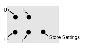
| Pin | Use |
|---|---|
| 1 | S1 Voltage + |
| 2 | S2 Voltage - |
| 3 | S3 Current +, S5 Store |
| 4 | S4 Current - |
| 5 | S[1-4] Common |
| 6 | S5 Store |
Front panel buttons.
Pin 1 is on the North end of the connector on the circuit board.
| Pin | Name |
|---|---|
| 1 | Positive |
| 2 | Negative |
| 3 | Ground |
When selecting an enclosure, you must actually layout the components before sizing the enclosure. Finding a good, cheap enclosure is a real PITA. There is no way to specify your size ranges and get a list of matching items. It doesn't help that there are no standard naming conventions; enclosure, junction box, instrument case, desktop, etc. all mean different things to each of the Asian suppliers.
I eventually found ST764 (7x3x5") DIY Hobby Electronic Metal Project Enclosure Box Case by Sunetec. When it arrived, the interior dimensions were actually slightly larger at 7.25" x 5.625" x 3.375".
At 195mm x 165mm x 90mm, this Blue Metal Enclosure Case DIY Power Junction Box (uxcell) for $14 from Amazon should have worked, but it was unavailable.
This enclosure also looked interesting, but with shipping it is fairly expensive.
As a perfectionist, the most stressful part of this project is cutting and drilling all of the holes in the enclosure! I tried to be careful, but soon it was obvious that it was impossible to not mar the paint, especially when using the sheet metal nibbler on the square holes. I resigned myself to repainting the enclosure when I was done.
The best way to make the edges of the rectangular holes straight was to use a flat bastard file. Using the Dremel here doesn't work well at all.
For voltage, 'U' seems to be the European preference and 'V' the preference in the U.S.. Therefore I chose 'V' for the front panel labels.
IEC 60320 C14 female connector (power socket) ripped from old computer PSU
fuse holder and 1A slow-blow fuse
power switch ripped from old computer PSU
large heat sink
PCB Mount Screw Terminal Block Connector, 3 pin, 2.54mm pitch (DC Power In)
PCB Mount Screw Terminal Block Connector, 2 pin, 3.5mm pitch (DC Power Out)
double binding posts (for banana jacks)
1 female D-Sub DE-9 serial connector
When the PC serial ports began to use 9-pin connectors, they were often mislabeled as DB-9 instead of DE-9 connectors.
The ATmega8 is programmed using a SPI (Serial Peripheral Interface).
I purchased the Sparkfun Pocket AVR Programmer which is an USB to SPI host adapter. See the Pocket AVR Programmer Hookup Guide.
One problem is that the power supply circuit board uses a non-standard 5 pin in-line interface instead of the standard 2x3 header.
I constructed a special cable for use with the Pocket AVR Programmer:
| Line | 1x5 pin | 2x5 pin |
|---|---|---|
| RST | 1 | 5 |
| MOSI | 2 | 1 |
| MISO | 3 | 9 |
| SCK | 4 | 7 |
| GND | 5 | 10 |
The 5V (PWR) line is not connected because the ATmega8 gets its 5V power from the circuit board.
Article 352 describes protection resistors for the MOSI, MISO, and SCK lines. But I believe that these are related to the fact that the article was describing a parallel port programmer interface, and that the Pocket AVR Programmer does not need such protection.
R3 is a 10KΩ pull-up resistor between the RST pin and the positive power supply which prevents the ATmega8 from accidentally entering programming mode.
Version 0.4.9 of the software was downloaded from the LinuxFocus article 389 download page.
- Hardware version 2.0
- Hardware version 3.0
- Design Guide for Rectifier Use
- Power Supply Basics for Effects
- Anatomy of Switching Power Supplies
- Atmel AVR on Wikipedia
The LinuxFocus site which hosts the original articles has not been updated since 2005-12-09, so I have local copies here:
- Part 1: The Hardware (LinuxFocus article 379)
- Part 2: The Software (LinuxFocus article 384)
- Part 3: Command and Control from the PC (LinuxFocus article 389)
- Programming the AVR microcontroller with GCC, libc 1.0.4 (LinuxFocus article 352)
- Button layout
These documents were delivered with the kit: